For decades, ultrafast lasers have been among the most powerful tools in modern optics. Their pulses last just a few hundred femtoseconds, or quadrillionths of a second, enabling technologies ranging from precision manufacturing and eye surgery to optical frequency combs, the Nobel Prize-winning innovation that powers the world’s most accurate optical atomic clocks.
Despite their importance, these lasers have largely remained large, costly systems that occupy entire optical tables.
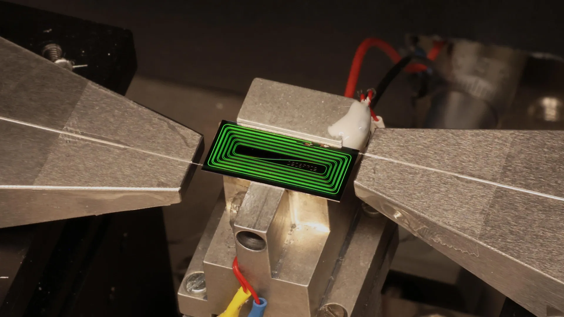
Now, researchers led by Professor Tobias J. Kippenberg at EPFL have achieved a breakthrough that could dramatically shrink the technology. Writing in Nature, the team reports the first integrated ultrafast laser capable of matching the performance of traditional tabletop femtosecond lasers. The device delivers pulse energies of 1.05 nanojoules and pulse durations as short as 147 femtoseconds, all from a photonic chip.
Bringing Ultrafast Lasers to Photonic Chips
Photonic chips manipulate light using microscopic structures called waveguides that are etched into a wafer. In much the same way electronic chips direct electrical signals, photonic chips guide and process light.
These chips are already widely used in telecommunications and have helped miniaturize many optical technologies that previously required much larger equipment.
“For more than twenty years, a high-pulse-energy femtosecond laser on chip was widely regarded as a holy grail of integrated photonics,” says Kippenberg. “Our result shows that it is not only possible, but that it can be achieved with a surprisingly elegant architecture that the integrated-photonics community had overlooked.”
An Overlooked Laser Design Delivers
To accomplish the feat, the researchers adopted a laser architecture known as the Mamyshev oscillator, a design that had received relatively little attention in integrated photonics.
The system places a nonlinear waveguide between two optical filters, each of which transmits a different portion of the light spectrum. As an intense laser pulse travels through the waveguide, it expands into a broader range of colors. Part of that broadened pulse can then pass through both filters and continue circulating within the laser cavity.
Weaker light behaves differently. Because it does not broaden enough, it is blocked by the filters and removed from the cycle.
“This design is especially attractive because it does not require any component that is difficult to make on this erbium-doped silicon nitride chip,” explains Zheru Qiu, a co-leading author of the paper.
According to Qiu, the design offers another major advantage. Photonic chips confine light to extremely small waveguides, causing light to interact strongly with itself. In many laser architectures, these nonlinear effects can destabilize the laser pulses. The Mamyshev oscillator, however, is far less susceptible to these problems, making it particularly well suited for integrated photonic devices.
Tiny Device, Big Potential
The laser cavity measures 42 centimeters in length, yet it can be folded onto a chip occupying roughly the area of a match head. This makes it dramatically smaller than conventional fiber-based ultrafast lasers.
Because photonic chips can be manufactured at wafer scale using methods similar to those employed for computer chips, more than 1,000 laser cavities could potentially be produced simultaneously. That manufacturing advantage could significantly reduce the cost of ultrafast lasers while expanding their availability for sensing, spectroscopy, and precision measurement applications.
“With kilowatt-level peak powers, the chip can drive demanding applications that have long depended on large, expensive laboratory lasers,” says Qiu.
The researchers believe the technology could eventually lead to portable and affordable devices for detecting environmental pollutants, identifying hidden defects in materials, and performing medical diagnostics. It could also help pave the way for compact optical atomic clocks that may play important roles in future communications and navigation systems.
The work involved researchers from the EPFL Institute of Electrical and Microengineering and Helmholtz-Zentrum Dresden-Rossendorf (HZDR).